
Services
PCB DESIGN

PCB designs for semiconductor, R&D centers. Providing double side and multi layer PCB with short delivery.
Application : Test Board, Failure analysis, Package conversion board
PCB thickness : 0.8 mm to 3.2 mm
Design : 1 day to 5 days, PCB making 3 days to 3 weeks.
Parts assembly capability : SMD pin pitch 0.4 mm
ATE BOARD DESIGN

Providing the probe card, Socket and PIB and DIB.
There are many different type of IC package with each having its own advantage and disadvantage. BGA and CSP use the ball of solder in grid pattern as connections to PCB. QFP and SOP are characterized by gull-wiring type lead. QFN and SON are no-lead, instead the electrode pad is prepared as terminal for connection.
CUSTOMIZED RACK

Rack specification : 15U to 42U / 19” to 23”
Option :
- Customized shelf
- Enclosure operation table
- KVM switch
- Swing monitor arm with keyboard tray
- Power Distributor
- Ground Bar
FIXTURE/MATERIAL FABRICATION

Design and material fabrication service for fixture.
Material: SUS, AL, Engineering Plastic, etc.
Plating: Baking finish, Anodized
Other: semi-auto, Full-Auto with Air, Motor drive
Application: Test fixture, JIG, Machine parts, ICT(In circuit Test) fixture
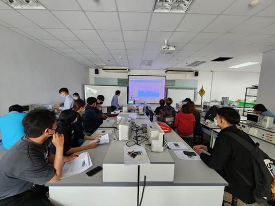
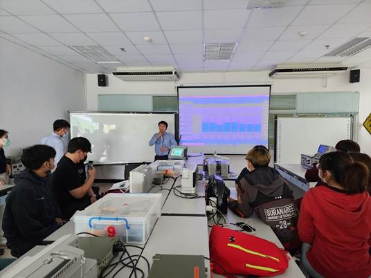
REPAIRING AND TRAINING


Demo & Training Anritsu “Spectrum Analyzer”